Innovation in photovoltaic technology is driven by the search for sustainable and effective energy production. In this study, we investigate how Anti-Reflective Coatings (ARCs) made of copper oxide nanoparticles (CuO NPs) might be integrated into Porous Silicon (PS) solar cells to increase photovoltaic efficiency. The main goal is to reduce incident sunlight loss from reflection, which will increase light absorption and energy conversion. Colloidal nanoparticles, or CuO NPs, were synthesized via the electrolysis process and coated onto glass substrates and p-type PS to create films through the use of the spin coating method. The Electrochemical Etching process (ECE) is used to prepare PS. X-ray Diffraction (XRD) and an Atomic Force Microscope (AFM) have been used to study the structural and morphological properties of copper oxide nanostructures (CuO NSs) that have been deposited on glass substrates, respectively. Scanning Electron Microscope (SEM) was investigated for CuO NSs. The optical properties of CuO NPs are studied. The photovoltaic characteristics of CuO NSs/PS/Si/Al solar cells were reporte and the efficiency of solar cells was calculated before and after the ARCs were added. The efficiency of PS/Si/Al solar cells is increasing from 0.268 to 2.97% after depositing CuO NPs.
Keywords
CuO Nanoparticles
Porous Silicon
XRD
Photovoltaic Efficiency
ARCs
Solar Cells
None
The definition of sustainable energy development is the growth of the energy sector in terms of producing, distributing and utilizing energy according to sustainability principles [1]. Energy systems in both industrialized and emerging nations will have a substantial impact on the environment. As a result, the world's sustainable energy system needs to minimize emissions and optimize efficiency [2]. Recent decades have seen a notable increase in the use of solar energy as a clean, sustainable power source. This is mostly because solar energy offers the ability to reduce environmental effects while meeting the world's expanding energy needs [3].
The optical losses in solar cells are a major concern in current photovoltaic science. In crystalline silicon solar cells, optical losses typically result in an efficiency loss of 7% [4]. As a result, the conversion efficiency of silicon solar cells may greatly benefit from a decrease in optical loss [5]. Anti-Reflection Coating (ARC) is essential for lowering reflection and minimizing optical loss, which raises the solar cells' conversion efficiency [6]. ARC uses the idea of phase variations in light and the relationship between reflectivity and refractive index to reduce reflection. Since the fabrication of the solar cell, numerous researchers have employed various ARCs and they are currently looking for a suitable ARC that can be utilized to increase the solar cell's efficiency [7,8].
PorousSilicon-(PS) is a-siliconcrystal with anetwork of spaces within it. A sponge-like structure of pores and channels encircled by a skeleton of crystalline silicon nanowires is produced by the nanosized gaps in the bulk siliconm [7,9]. PS solar cells have become a viable option for effective photovoltaic energy generation in the field of solar energy conversion technologies [10]. Cost-effectiveness, simplicity of manufacture and compatibility with large-scale production techniques are only a few benefits of porous silicon [11,12]. Scientific communities have been very interested in the coupling system made up of semiconductor Nanocrystals (NCs) and metal nanoparticle NPs [7].
Transitional metal oxides, including ZnO, CuO, TiO2, Fe3O4 and NiO nanoparticles, have demonstrated effective applications as advanced nano-substances in the fields of energy, biology and the environment [13]. Because of their electrical, magnetic, optical and physical properties, copper oxide nanoparticles (CuO NPs) are particularly interesting among the oxides of transition metals [14] and they will used as ARC in this work.
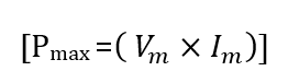
The power produced by the solar cell can be calculated along with the I-V diagram by using the equation (P=IV), at the short circuit current (Isc) and open circuit voltage (Voc) points. Figure 1 shows the voltage and the current at this maximum power point are denoted as Vm and Im respectively [15].
The FillFactor (F.F.)is an imported measure of thequalityof the solar cell. It is calculated by comparing the maximumpower (Pmax) tothe theoretical power (PTh= Voc´Isc, as given in the following equation [17]:
(1)
Efficiency(η)is the ratioof the outputelectricalpower(Pout) to thesolarinputpower (Pin) in the PV cell. Pout can be taken to be
sincethesolar cell can be operated up toits maximumpoweroutput toget themaximumefficiency [18]:
(2)
Efficiency is related to current density Jsc and Voc usingF.F as the following equation:
(3)
Figure 1: Maximum Power on I-V diagram of Si solar cell [16]
Figure 2: (a) the setup of the ECE process (b)PS image
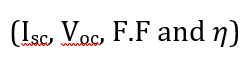
These four quantities
arethekeyperformancecharacteristicsof asolarcell.
Experimental Work
CuO NPs are produced by the simple chemical process known as electrolysis, which has been used in earlier research [9]. For this, the electrolysis cell is employed, a gold plate serving as the positive electrode and a copper plate serving as the negative electrode of the electrolysis’ cell, with dimensions (3, 2 and 0.2) cm in length, width and thickness, respectively for each electrode. DC voltage of 5 volts is connected in series with the cell's anode. The electrolyte liquid used was water mixed with Hydrochloric Acid (HCl) at a ratio of roughly 8:1 and the procedure took about 25 minutes [8].
Spin coating was used to create CuO NSs thin films, the centripetal force produced by spinning movement helps to form a homogenous layer. Thin coatings can be deposited on flat substrates (2 cm * 2.5 cm) made of glass and PS at the end of this group production procedure. By depositing and spinning a viscous film at a high speed (about 3000 rpm), the film is forced to spread across the substrate. To remove residue and impurities, glass substrates were cleaned with alcohol in an ultrasonic bath at the beginning.
ECE process was performed to produce PS. Wafers of p-type silicon with an orientation (100), a thickness of 508 μm and a resistivity of 4 to 20 (ohm. cm) are used. The etching solution, contained in a Teflon cell, is a mixture of HF (48%) and ethanol (99.99) in equal proportions, with a current density of 10 mA/cm² applied for ten minutes at room temperature. Utilizing a gold ring as a cathode, the current traversed the electrolyte from the rear surface to the upper surface, resulting in the formation of an etched region on the silicon sample of 0.785 cm², as illustrated in Figure 2. The samples were stored in a plastic container containing methanol to prevent oxidation of the PS surface.
X-ray diffractometer supplied by SHIMADZU, XRD-6000 was used to get X-ray diffraction pattern of PS and CuO NSs. It uses Cu Kα radiation line of wavelength of 1.54 Å in 2Theta ranging from 20° to 80°. The morphology of the CuO NSs examined by atomic force microscopy (AA 3000 Scanning Probe Microscope. FESEM studies have been done on TESCAN, Czech Republic, JSM-6335F. The OPTIMA, SP 3000 UV-VIS spectrophotometer was used to record the absorption spectrum of the CuO NPs, which covered a wavelength range (200-1100) nm.
RESULTS AND DISCUSSION
The X-ray diffraction pattern of CuO NSs is shown in Figure 3, it illustrates the crystalline particles by the peak corresponding to standard Brag reflections (111) at an angle equal to 38.1554°. The CuO NSs had a monoclinic crystal structure. The broadening of the peak at this angle is proof that monocrystalline copper oxide was formed. The inset chart illustrates the XRD pattern of the p-type PS layer. It showed a monocrystalline structure, with strong peak broadening corresponding to the diffraction angle (69.28°), which is interpreted as a nanocrystalline size effect.
Byusingthewidth ofa peakwhichappears at theangleon the2θ scale inScherer law [8]:
(4)
Table 1: The values of the grain size, FWHM, strain (d), and the dislocating density η of CuO NSs and p-type PS
Material
2θ (Deg)
FWHM (Deg)
D (nm)
δ* 10^14 lines/m^2
η*10^-4 (lin-2m-4)
CuO NSs
38.1554
0.2084
40.33
6.15
8.19
PS
69.2805
0.1100
87.75
1.287
3.94
Table 2: The values of the CuONSs' average diameter, roughens average and root mean square
Material
Avg. Diameter (nm)
Roughens average
Root mean square (nm)
CuO NSs
78.07 nm
2.92
3.38
Figure 3: The XRD pattern of CuO NSs and the inset chart XRD of p-type PS
Figure 4: AFM image of CuO NSsand distribution chart
where, D is the grain size, β represents the Full Width At Half Maximum (FWHM) in degrees and θ is the diffraction angle, the size of the generated CuO NSs was 40.33 nm and 87.75 for PS. Microstrainvalue (d)andthedislocatingdensity(η) values are measured by using the following equations [8] (Table 1):
(5)
(6)
Figure 4 illustrates the surface morphology of CuO NSs, which was investigated using AFM and possesses exceptionally smooth and homogeneous structures. The average grain size is approximately 78 nm using software and AFM analysis (Table 2).
The FTIR spectrum of CuO NPs formed by electrolysis is shown in Figure 5. The important bands of absorbance at peaks (3430.32,1630.42 and 558.00) cm-1 are displayed in this figure. The O-H expansion pattern of the hydroxyl group is related to the broad absorption peak at around 3430.32 cm-1 because a high surface-to-volume ratio in CuO NPs therefore it absorbs moisture. It is brought on by the adsorbed water molecules and this is agreed with other researchers [19]. While the C=O band is associated with the band in the range 1630.42cm-1. The stretching vibration of the Cu-O bond is responsible for the high absorption band at 558 cm-1.
Figure 6 shows the FESEM image of CuO NSsdepositedon a glasssubstrate. It is observed that the morphology of the CuONSs was mostly spherical i with a tiny size range from (20.47 to 33.50) nm.
The optical range gap of a material can be better understood in terms of its electrical nature by studying UV-VIS absorption spectroscopy. Figure 7 shows the absorption spectra of CuO NPs, with the absorption edge around 315 nm suggesting that associated electron processes within the sample are responsible for near-ultraviolet absorption. It was concluded that the material is effective because it has strong absorption in a UV range of 316 nm.
Figure 5: FTIR spectrum of CuO NPs
Figure 6: FESEM image of CuO NSs
Figure 7: UV-VIS absorption spectrum of CuO NPs
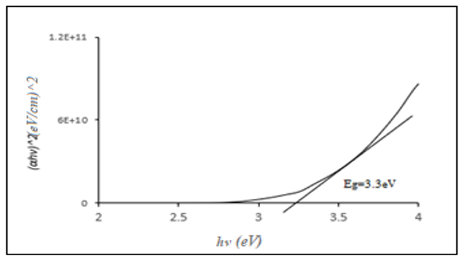
The energy band gaps of CuO NPs, according to a mathematical model, the square of (α hυ) is plotted against (hυ). The straight line is extrapolated to (αhυ)2 =0 and it results in the value of the energy gap as shown in Figure 8. The value of the optical band gap of CuO NPs is about 3.3eV due to the direct band-to-band transition. The increase in the energy gap is due to nano-sized particles being formed and this is backed by AFM and FESEM.
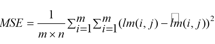
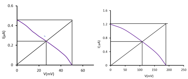
Figures (9a and b) show the open-circuit voltagewhentheloadresistanceisgreaterthanthedeviceresistanceandthecurrentvalueiszeroofthesolarcells (PS/p-Si/Al and CuO NSs /PS/p-Si/Al) respectively. From these figures, it can be calculated the values of Voc, Isc, Vm and Im.Byusingequations1and2, it can be calculated thevaluesof fillfactors and the efficiencies of thesesolarcellsrespectively. All samples were tested under the illumination of a light source with a light intensity of (33mW/cm2).
Figure 8: (αhν)2 versus hv of CuO NPs
Figure 9: The efficiency0of (a) 0PS/p-Si/Al solar cell and (b) 0CuONSs/PS/p-Si/Al solar cell
Table 3: The values of the photovoltaic characteristics of PS/p-Si/Al solar cells with and without adding the CuO NPs
Isc00
0Voc 0 (mV) 00
Im0
0Vm0
Solar cells
(µA) 0 0
(µA) 00
(mV) 00
F.F%00
Efficiency%
PS/p-Si/Al
0.45
50
0.24
29
30.9
0.268
CuO NPs/PS/p-Si/A
1.2
190
0.7
110
33.7
2.97
The enhancement in efficiency can be interpreted as that the CuO NSs, act as an anti-reflected layer covering the porous silicon solar cells, increasing the absorption ratio of the light, thus reducing the reflection losses in PS/Si/Al solar cells.
It is clear from the results illustrated in Table 3 that the solar cells of PS/p-Si/Al prepared at etching time (10 min) have low efficiency equal to 0.268%, but this value is enhanced after depositing CuO NPs. It increased to 2.97%. The enhancement in efficiency can be interpreted as the CuO NSs acting as an anti-reflected layer covering the porous silicon solar cells led to an increase in the absorption ratio of the light, thus reducing the reflection losses in PS/Si/Al solar cells.
CONCLUSION
CuO NPs were successfully synthesized using the electrolysis method. The CuO NPs were deposited onto the glass substrates and porous silicon substrates using the spin coating technique. This method allowed for the formation of a uniform and controlled thin film, essential for optimizing the anti-reflective properties of the coating. The nanoparticles demonstrated remarkable optical characteristics due to their homogeneous dispersion and tiny size. CuO NPs greatly decreased the surface reflectance of Porous Silicon (PS) solar cells when used as an anti-reflective coating, enabling higher light absorption. This resulted in a measurable improvementin theefficiencyof the CuO NSs/PS/Si/Al solar cells. CuO NPs' simplified synthesis and low cost, combined with their ability to improve light capture, show that they have potential as a material for photovoltaic applications.
REFERENCES
Golušin, M., et al. "Sustainable Energy Management Prerequisite for the Realization Kyoto Protocol." Journal of Economic Development, Environment and People, vol. 1, no. 2, 2012, p. 24.
Salvarli, M.S. and H. Salvarli. "For Sustainable Development: Future Trends in Renewable Energy and Enabling Technologies." Renewable Energy-Resources, Challenges and Applications, edited by IntechOpen, 2020.
Maka, A. and J. Alabid. "Solar Energy Technology and Its Roles in Sustainable Development." Clean Energy, vol. 6, no. 3, 2022, pp. 476–483.
Fahim, N., et al. "Efficiency Enhancement of Screen-Printed Multicrystalline Silicon Solar Cells by Integrating Gold Nanoparticles via a Dip Coating Process." Optical Materials Express, vol. 2, no. 2, 2012, pp. 190–204.
Park, H., et al. "Improvement on Surface Texturing of Single Crystalline Silicon for Solar Cells by Saw-Damage Etching Using an Acidic Solution." Solar Energy Materials and Solar Cells, vol. 93, no. 10, 2009, pp. 1773–1778.
Hiller, J.A., et al. "Reversibly Erasable Nanoporous Anti-Reflection Coatings from Polyelectrolyte Multilayers." Nature Materials, vol. 1, no. 1, 2002, pp. 59–63.
Khalifa, M., et al. "Quantum Dots Gold Nanoparticles/Porous Silicon/Silicon for Solar Cell Applications." Materials Today: Proceedings, vol. 45, 2021, pp. 5809–5814.
Khalifa, M., et al. "Al₂O₃ NPs/Porous Silicon/Silicon Photovoltaic Device." Journal of Physics: Conference Series, vol. 1853, no. 1, IOP Publishing, 2021, p. 012046.
Basu, S. and J. Kanungo. "Nanocrystalline Porous Silicon." Crystalline Silicon-Properties and Uses, 2011, pp. 219–250.
Gohar, O., et al. "Nanomaterials for Advanced Energy Applications: Recent Advancements and Future Trends." Materials & Design, vol. 241, 2024, p. 112930.
Razykov, T. M., et al. "Solar Photovoltaic Electricity: Current Status and Future Prospects." Solar Energy, vol. 85, no. 8, 2011, pp. 1580–1608.
Green, M.A. "Solar Cell Efficiency Tables." Progress in Photovoltaic Research and Applications, vol. 8, 2000.
Pakzad, K., et al. "Green Synthesis of Ni@Fe₃O₄ and CuO Nanoparticles Using Euphorbia Maculata Extract as Photocatalysts for the Degradation of Organic Pollutants under UV-Irradiation." Ceramics International, vol. 45, no. 14, 2019, pp. 17173–17182.
Lanje, A. S., et al. "Synthesis and Optical Characterization of Copper Oxide Nanoparticles." Advances in Applied Science Research, vol. 1, no. 2, 2010, pp. 36–40.
Wolfe, P.R. "What Is Photovoltaics?" 2018.
Aernouts, T. "Organic Bulk Heterojunction Solar Cells: From Single Cell Towards Flexible Photovoltaic Module." 2006.
Chan, D., et al. "A Comparative Study of Extraction Methods for Solar Cell Model Parameters." Solid-State Electronics, vol. 29, no. 3, 1986, pp. 329–337.
Krc, J. Optical Modeling and Simulation of Thin-Film Photovoltaic Devices. CRC Press, 2013.
Radhakrishnan, A.A. and B. B. Beena. "Structural and Optical Absorption Analysis of CuO Nanoparticles." Indian Journal of Advanced Chemical Science, vol. 2, no. 2, 2014, pp. 158–161.
Recommended Articles
Research Article
OBSERVATIONS ON THE HOMOGENEOUS TERNARY QUADRATIC DIOPHANTINE EQUATION x2 + 4xy + 9y2 = 21z2
Download PDF
Research Article
Computer Driven Library Management and Service Rendering System: Mobile Library Landscape
Yekini N. A,
...
Ojo O
Published: 10/06/2020
Download PDF
Research Article
Influence of Optimum Percentage of Waste Ceramic Powder as a Fine Aggregate Replacement on Hardened Properties of Concrete
Mohammad Ali Asaad,
...
Mohammed Muhsin
Published: 11/06/2020
Download PDF
Research Article
The Possibility of Treating Corrosion in Iron Valves of Flow Regulators, Pumping Station Components, and Suspended Solids Filtration Networks in Rivers and Streams in Al-Qadisiyah Governorate
Qasim M. Turki,
...
Ahmed Hakem Jabor
Published: 02/03/2026
Download PDF
PO Box 101, Nakuru
Kenya.
Email: office@iarconsortium.org
Editorial Office:
J.L Bhavan, Near Radison Blu Hotel,
Jalukbari, Guwahati-India
J. Khalifa, M. & Ahmed Khalaf, A. (2025). Enhancing Photovoltaic Efficiency of Porous Silicon Solar Cells with Copper Oxide Nanoparticle Anti-Reflective Coatings. IAR Journal of Engineering and Technology, 6(1), 1-6.
MLA
J. Khalifa, Manal and Abdulla Ahmed Khalaf. "Enhancing Photovoltaic Efficiency of Porous Silicon Solar Cells with Copper Oxide Nanoparticle Anti-Reflective Coatings." IAR Journal of Engineering and Technology 6.1 (2025): 1-6.
Chicago
J. Khalifa, Manal and Abdulla Ahmed Khalaf. "Enhancing Photovoltaic Efficiency of Porous Silicon Solar Cells with Copper Oxide Nanoparticle Anti-Reflective Coatings." IAR Journal of Engineering and Technology 6, no. 1 (2025): 1-6.
Harvard
J. Khalifa, M. and Ahmed Khalaf, A. (2025) 'Enhancing Photovoltaic Efficiency of Porous Silicon Solar Cells with Copper Oxide Nanoparticle Anti-Reflective Coatings' IAR Journal of Engineering and Technology 6(1), pp. 1-6.
Vancouver
J. Khalifa M, Ahmed Khalaf A. Enhancing Photovoltaic Efficiency of Porous Silicon Solar Cells with Copper Oxide Nanoparticle Anti-Reflective Coatings. IAR Journal of Engineering and Technology. 2025 Jan;6(1):1-6.



 Download PDF
 Download XML