The objective of the research project is to develop nanocrystalline Porous Silicon (PSi) coating through the electrochemical etching on the research neuro-type silicon substrates. In identifying the size and structure of nanoscale properties, the X-ray diffraction analysis, Fourier-transform infrared spectroscopy and atomic force microscopy have been entirely employed to characterize the produced material in nanoscale. Synthesis of colloidal nanoparticles involved electrolytic reaction with the alumina nanoparticles (Al2O3) and preparation of the alumina nanoparticles as a thin film was done by drop-casting technique. The nanoparticles of Al2O3 were studied in an appropriate manner in terms of their morphology, structure and optical properties. It was disclosed that when these nanoparticles were incorporated in the porous silicon photovoltaic system, the solar cell system of Al2O3/PSi/Si/Al had phenomenal results concerning the performance indicators of the system.
Keywords
Nanostructured Porous Silicon
Nanoparticles of Alumina
Photovoltaic Devices
X-Ray Diffraction
UV- Visible Spectroscopy
Atomic Force Microscopy
Infrared Spectroscopy
INTRODUCTION
In the last several decades, the study of nanomaterials has experienced a remarkable increase in scientific community, mostly due to the typical physical behaviors which are so separated in comparison to the bulk materials and isolated atoms [1]. Nanoscale materials possess quantum confinement properties, large surface-volume ratio as well as high reactivity compared to bulk materials. These fundamental changes in the material behavior have offered novel opportunities in technological advancement in many aspects. The quantum mechanical properties that become available when dimensions are less than 100 nanometers and cannot be implemented using conventional materials offer new capabilities. Surface plasmon resonance, quantum tunneling effects and changed electronic band structures are the overriding forces that determine the properties of materials at this scale. The metal oxide nanoparticles have become versatile commodity in the uses in catalysis, sensing, semiconductor devices, biomedical devices [2], energy storage and capacitor devices [3].
Aluminum oxide in the various shapes that are found in the nature is one of the most abundant and at the same time the number of things that have been known in history [4]. The outstanding provisions of the Al2O3 , its use in optoelectronic work, which is especially inviting as regards the use of this substance as a high-quality gate dielectric material. It contains one of the greatest refractive index, amazingly the ability to endure the severe environmental circumstances in addition to the high optical clarity, which qualifies it to be an ideal candidate to the high-tech electronic uses [5]. Al2O3 is also observed to have other important properties; low permeability, good thermal conductivity, high mechanical rigidity and good thermal and chemical stability which make alumina nanoparticles very versatile in realising photovoltaic devices where they may be used in a variety of different ways: as passivation layers to minimise surface recombination, as anti-reflection coating to couple light into a device more efficiently and as charge-selective contacts to extract carriers better out of a device, all can be approached by nanoparticles [6,7].
The most common material in microelectronic fabrication is still crystalline silicon or (c-Si), however, with a quite limited indirect bandgap of approximately 1.12 eV, which is a drawback in certain applications, the indirect bandgap character causes photon absorption to be assisted by phonons, which reduces its absorption coefficients relative to direct bandgap semiconductors. This means that rather thick silicon layers (usually 150-300 µm) are needed to collect enough sunlight to convert it into energy efficiently. [8]. Porous silicon PSi is a kind of nanostructured matrix which is composed of interconnected pore voids along with tiny columns of silicon crystallites of nanometers in diameter [9]. Gives the building an unusually high internal surface area of 500 m²/cm³. The technology of PSi production is based on a simple and low cost electrochemical etching of c-Si substrates in the solutions of HF acids [10]. The reflection coefficient of PSi can be reduced to below 5% across the visible spectrum, compared to approximately 35% for polished silicon surfaces. Electrically, the large surface-to-volume ratio introduces a high density of surface states that can significantly affect charge carrier dynamics. Surface recombination velocities in untreated PSi can reach 10⁵-10⁶ cm/s, must possess good passivation in order to reduce losses of carriers. The evolution of the production of optical elements on the substrate of PSi layers and silicon optoelectronic devices presuppose the profound understanding of the electrical peculiarities of the technology. The optical, electrical and electronic properties vary greatly upon the reduction of the bulk silicon to nanoscale in porous structures [8]. The evolution of optical aspects in PSi layers deposited on silicon substrate and the optoelectronics devices involves the profound knowledge of electrical characteristics of this technology [11,12].
MATERIALS AND METHODS
Synthesis of Alumina Nanoparticles
Colloidal Al₂O₃ nanoparticles were prepared in a configuration of an electrolytic cell. The anode electrode was made up of an aluminum plate (anode) and a layer of gold (cathode) of area (3×2×0.2) cm. The anode was hooked up sequentially with a DC supply of 5 volts. Hydrochloric acid (HCl) aqueous solution at 8:1 ratio of water to acid was the medium of electrolyte. The electrolysis reaction was carried out in 30 minutes, the products of the reaction were the electrolysis products of colloidal Al₂O₃ nanoparticles which were deposited on glass substrates (2 cm × 2 cm) through the drop-casting method to form thin films.
Fabrication of Porous Silicon
Wafers of p-type crystalline silicon with resistivity of 4-20 Ω cm3, crystal thickness of 508 00 and (100) crystal orientation were utilized as bottom substrates. The size of the substrate was (2x2) cm2. Electrochemical etching was performed using a 1:1 mixture of HF (48%) and ethanol (99.99%) at ambient temperature with a gold (Au) electrode. A current density of 10 mA/cm² was maintained for 10 minutes, producing an etched region of approximately 0.785 cm².
Characterization Techniques
A SHIMADZU XRD-6000 diffractometer was used to obtain the patterns X-ray of diffraction of the Al₂O₃ thin films and PSi structures. The measurements used the 1.54 A Cu Kalpha radiation, which was scanned over the 20° to 80° 2θ range.
An OPTIMA SP-3000 UV-VIS spectrophotometer with the spectral range of 200-1100 nm was used in recording the optical absorption and transmission spectra.
The surface morphology studies were performed with the help of an AA 3000 Scanning Probe Microscope (Atomic Force Microscopy mode) to identify the distribution of particle size and the topography of surfaces of the obtained althin films and PSi structures.
RESULTS AND DISCUSSION
Structural Characterization by X-ray Diffraction
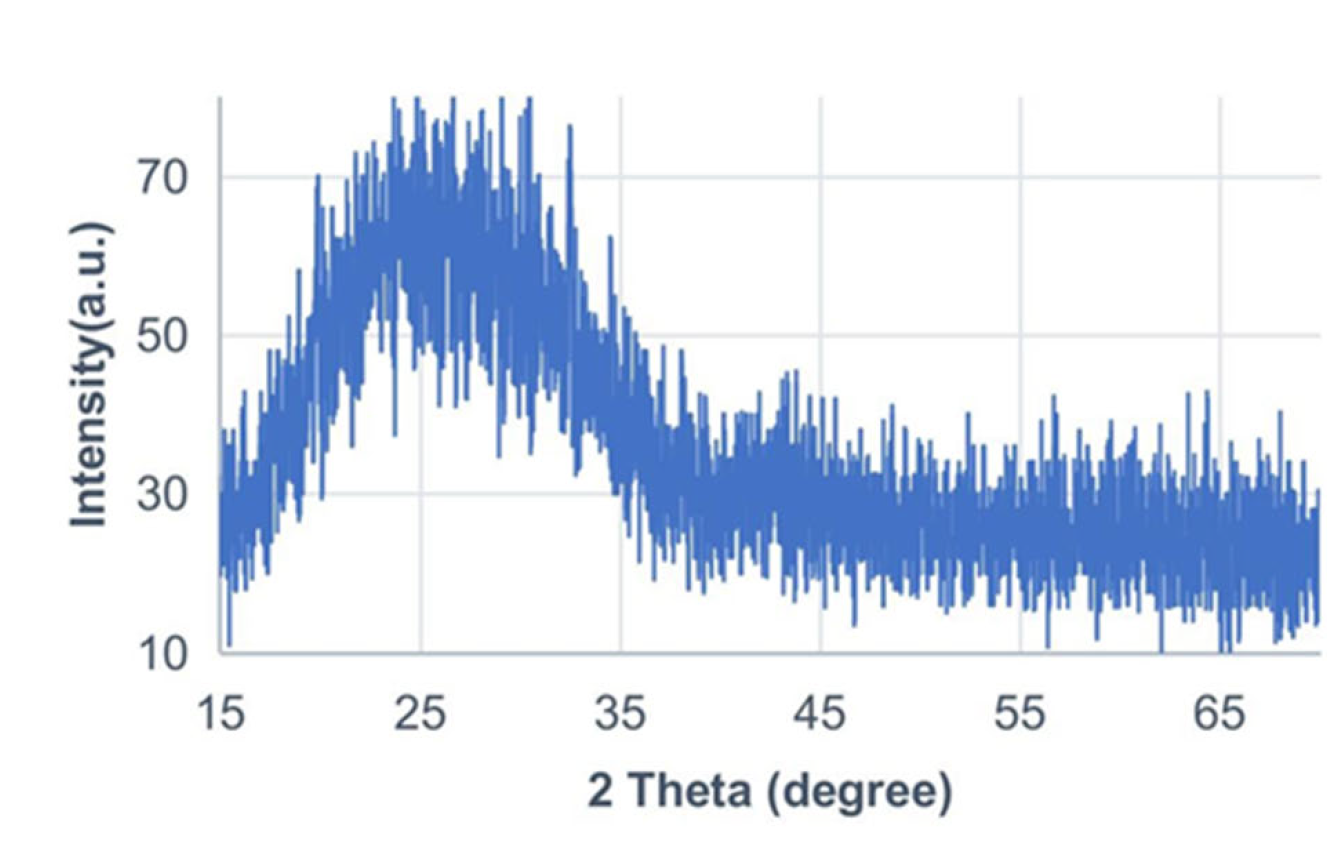
Figure 1 and Figure 2, x-ray diffraction measurements of the synthesized Al₂O₃ thin films and PSi were carried out with the use of the Cu K α radiation (λ = 1.543 Å). The diffraction pattern showed broad peaks of characteristics of nanostructured materials. The result of the XRD pattern of Al₂O₃ was indexed against the standard JCPDS file no. 36-1457.
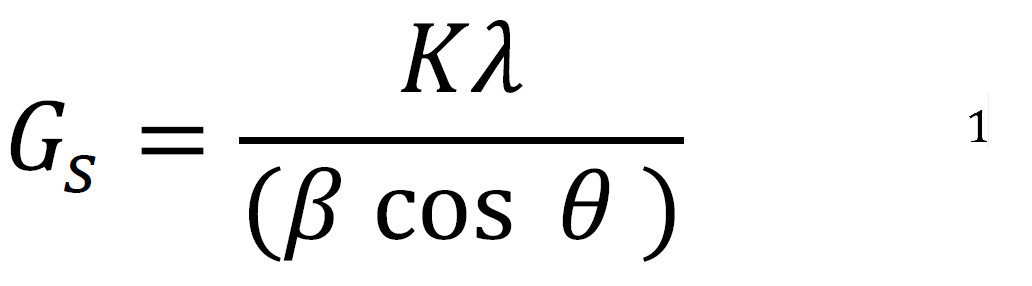
The Scherrer equation was used to compute the crystallite size [13]:
1
Figure 1: "The XRD Pattern of Al₂O₃ Thin Film
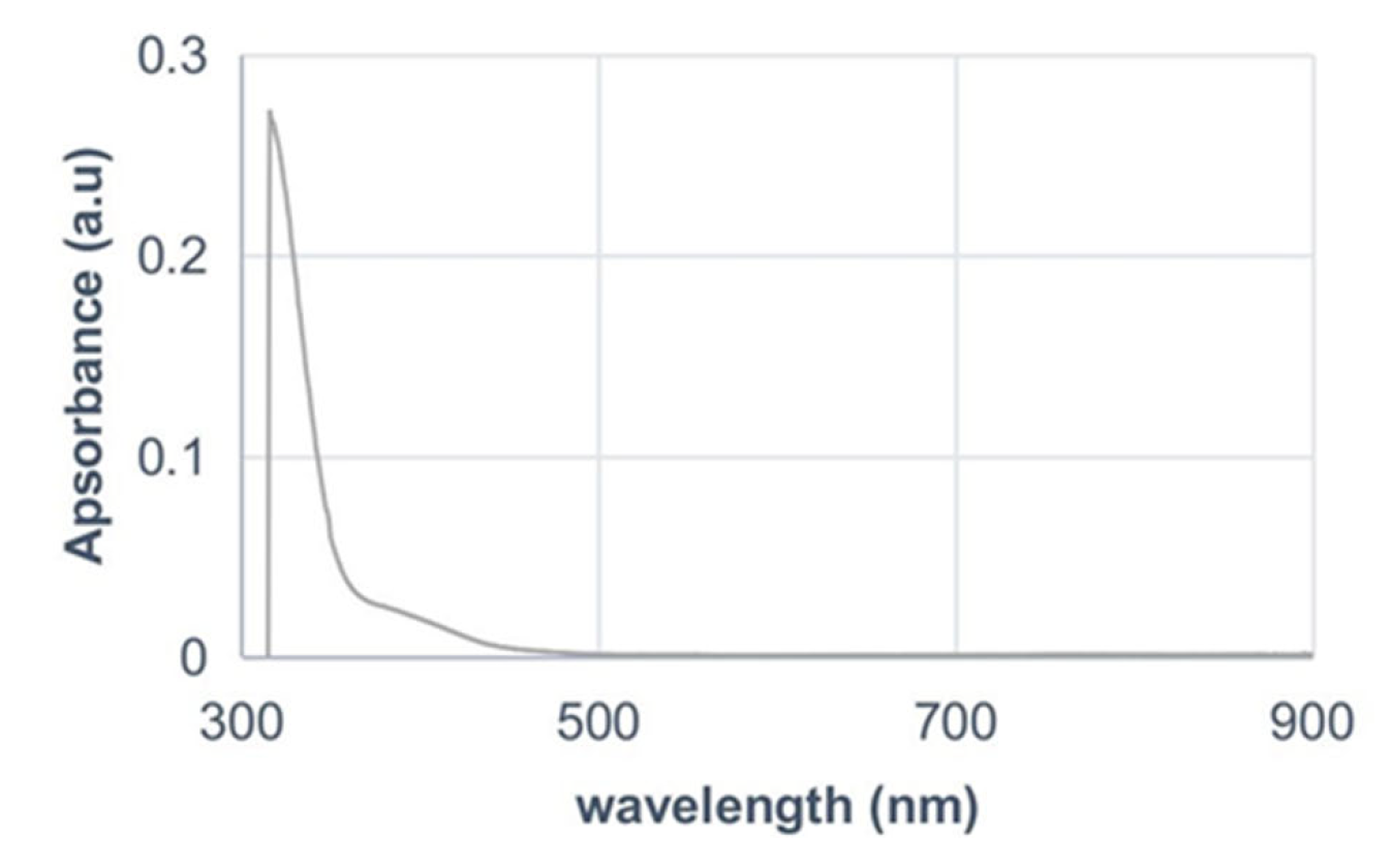
Figure 2: UV-VIS Absorption Spectrum of Al₂O₃ Nanoparticles
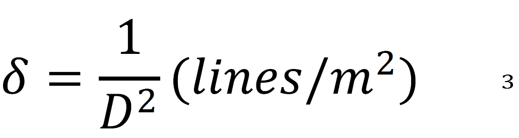
In which Gs will be the crystal size, K will be the shape factor (considered to be 0.9), λ will be the X-ray wavelength, β will be the Full Width Half-Maximum (FWHM) in radians and θ will be the Bragg diffraction angle. Based on the peak of 2 θ = 19.876°, the size of nanocrystallites was calculated to be approximately 20 nm. The broadening of diffraction peaks observed in the XRD pattern is characteristic of nanocrystalline materials and arises from two primary sources: finite crystallite size (size broadening) and lattice strain (strain broadening) (Table 1).
Table 1: Structural Parameters of Al₂O₃ Thin Film
2 θ (deg)
FWHM (deg)
GS (nm)
δ × 10¹⁴ (lines/m²)
η × 10⁻³
19.876
0.411
20.531
23.70
1.7613
The equations 2 and 3 were used to find the values of microstrain (η) and dislocation density (δ) [14,15]:
Optical Properties Analysis
UV-Visible Absorption Analysis: UV-visible absorption spectroscopy is of use in the study of electronic structure and optical bandgap of materials. Absorption spectrum of Al₂O₃ indicates that there is an absorption edge of approximately 350 nm that represents near-ultraviolet absorption is due to an electronic transition in the sample.
The absorption edge of 350 nm (approximately 3.54 eV) is also blue-shifted relative to bulk Al₂O₃ which would normally have an absorption onset in the deep UV region because of its large bandgap (6.2-8.7 eV by phase).
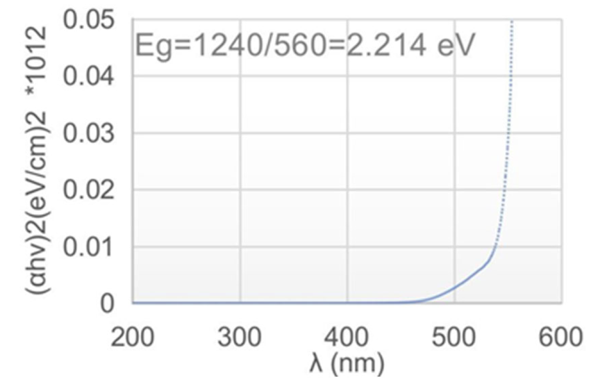
The plot (α h ν)² vs photon energy (hν) was used to determine optical bandgap energy of Al₂O₃. Where the α symbolizes the absorption coefficient. The linear part of the curve was extrapolated to the axis of photoelectron energy to measure the bandgap measurement which was 2.214eV. The Tauc plot analysis (i.e., (α h ν)² vs photon energy) would be appropriate to analyze bandgap of allowed direct transition. The linear relationship between the Tauc plot is an indication that there is the direct transition behavior of the absorption edge but the bulk of Al₂O₃ has the direct transition behavior which is generally described as an indirect transition behavior (Figure 3).
Figure 3: (α h ν)² Versus Photon Energy Plot for Bandgap Determination
Surface Morphology by Atomic Force Microscopy
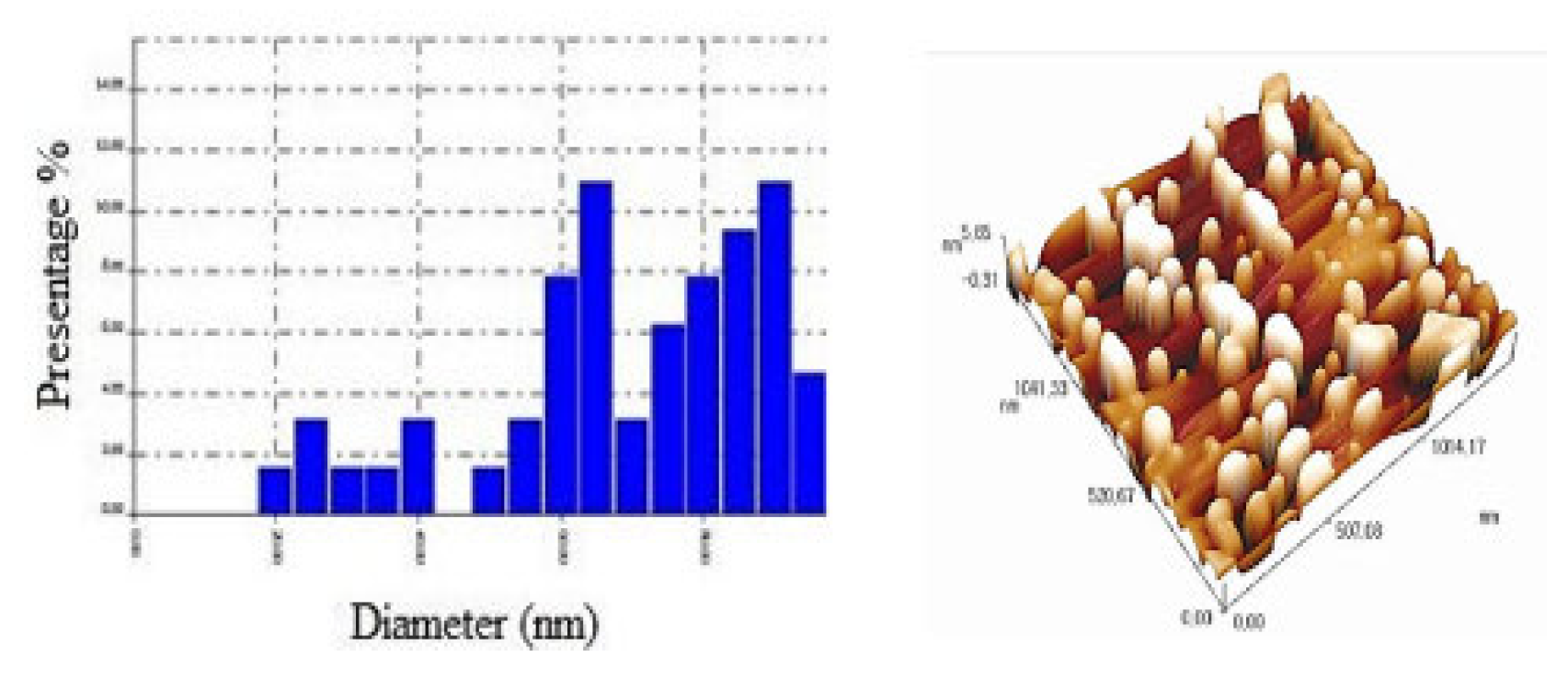
As far as AFM analysis is concerned, the homogenous and smooth structural properties of the Al₂O₃ surface were found.
The average grain size according to the AFM data which was identified as about 74.52 nm was determined by the results of the analysis software (Figure 4).
Figure 4: 2 D and 3 D AFM Images of Al₂O₃ Thin Film
The AFM scan provides a lot of information concerning the morphology of the deposited film of Al₂O₃. The obtained AFM outcome of 75 nm on the average grain size is larger as compared to the size of the crystallites of approximately ~20 nm in the XRD analysis. This apparent inconsistency is not as strange as it sounds and can be attributed to the different physical quantities which are measured by each of those methods (Table 2).
Table 2: Surface Morphology Parameters of Al₂O₃ Thin Film
Average Diameter (nm)
Average Roughness (nm)
Root Mean Square (nm)
75.1
1.62
1.825
Electrical Characterization of Heterojunction
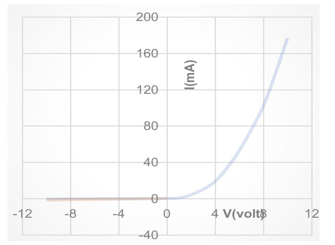
Dark Current-Voltage Characteristics: Dark I-V characterization of Al2O3/PSi/Si heterojunctions on forward and reverse bias was investigated. The current was observed to be extremely limited at applied voltages that were less than 1 volt in forward bias that indicates that there were potential barriers at the heterojunction interface.
The dark I-V characteristics provide fundamental information about the charge transport mechanisms and barrier properties of the heterojunction (Figure 5).
Figure 5: Dark I-V Characteristics of Al₂O₃/PS/Si Heterojunction
Photocurrent Response Under Illumination
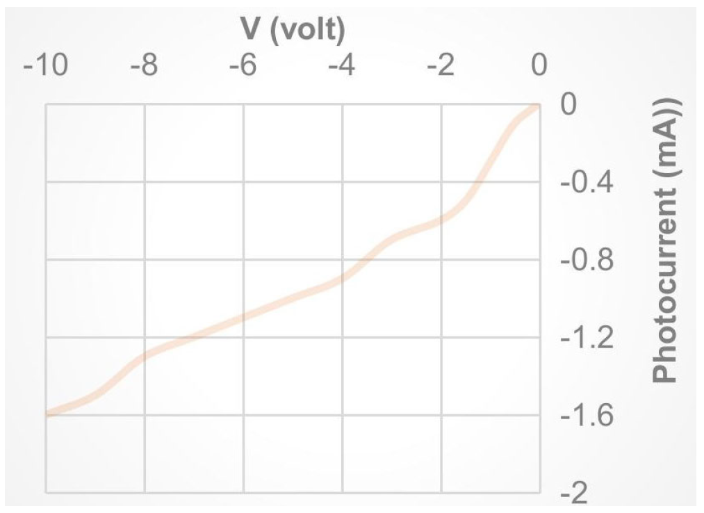
The photovoltaic characteristics of the solar cells are important parameters since they directly determine the ability of the solar cell to convert the incident optical energy into electrical current. Under the high illumination conditions especially in reverse-bias conditions, the photocreation of electrons and holes in the depletion region is increased as the photocurrent is created in the first place.
These enlightened currentvoltage (IV) characteristics give a graphic representation of the photoresponse of the device and leaves no question that the device still has another piece of irrefutable evidence of the successful photovoltaic behavior. The tendency of the activity of photodiodes to the dominance of photocurrent in the conditions of reverse-biasing of the diode is due to the fact that the influence of the separation of the charge carriers is activated by the built-in electric field. The silicon material creates its pairs of electrons and holes in case of incident light absorption. The carriers produced even in the depletion region and even the carriers produced directly in the diffusion length of the depletion region, would be in effect repelled by the internal electric field: holes would be repelled towards the p-type region and electrons towards the n-type contact. This directed flow of charge carriers results in the production of a photocurrent that is appreciably large (Figure 6).
Figure 6: Illuminated I-V Characteristics of Al₂O₃/PSi/Si Heterojunction
Solar Cell Performance Parameters
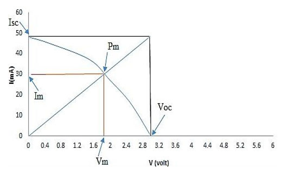
There were significant improvements in the open-circuit voltage (Voc, measured at R = ∞, I = 0) and short-circuit current (Isc) (Figure 7).
Figure 7: Light Up I-V Characteristics of the Full Ag/Al₂O₃/PSi/Si/Al Solar Cell Structure
The improvement in Isc as well as Voc led to an increase in the output power in turn leading to the overall efficiency of the solar cell using Al₂O₃ nanoparticles. The parameters of solar cell Al₂O₃/PSi/Si, as presented in Table 3.
Table 3: Performance Parameters of Al₂O₃/PSi/Si Solar Cell
I_sc (mA)
Voc (V)
Im (mA)
Vm (V)
F.F (%)
η (%)
50
2.95
30
1.86
37
12.0
The solar cell efficiency (η) is computed as:
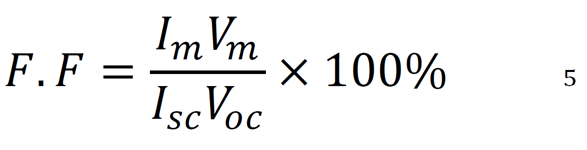
The fill factor (F.F) is calculated as:
Where Im, Vm denote the current and the voltage at maximum power point.
The achieved efficiency of 12% represents a significant accomplishment for a porous silicon-based solar cell incorporating alumina nanoparticles.
CONCLUSION
The paper could bring out the synthesis of colloidal Al₂O₃ nanoparticles through the process of electrolytic process and deposition of these particles on the glass surfaces through the drop-casting method. It is an easy way of deposition that is low cost compared to other complicated fabrication processes. When electrochemical etching of P-type silicon substrates was employed, then Al₂O₃/PSi/Si heterojunction was obtained. Al₂O₃deposited films were found to be optically transparent over the spectral region of 360 to 900 nm. The electrical characteristics of the heterojunction device were also highly enhanced, which was due to the optimum bandgap engineering through the integration of nanomaterials. The efficiency of solar cells is significantly enhanced and it has been found that the nanoparticles of this type can be incorporated into the porous silicon structure quite successfully and an exit to the further evolution of solar cell technologies is offered. It was found to be 12 % with an open-circuit voltage of 2.95 V and this has shown the potential of this method to be very great in the development of the next generation of high-performance photovoltaic devices.
REFERENCES
Muralidharan, V.S. and A. Subramania. Nanoscience and Technology. 2009, pp. 542.
Dalla Pria, P. “Evolution and new application of the alumina ceramics in joint replacement.” European Journal of Orthopaedic Surgery & Traumatology, vol. 17, 2007, pp. 253–256.
Dillon, A.C. et al. “Metal oxide nanoparticles for improved electrochromic and lithium-ion battery technologies.” Thin Solid Films, vol. 516, 2008, pp. 794–797.
Piriyawong, V. et al. “Preparation and characterization of alumina nanoparticles in deionized water using laser ablation technique.” Journal of Nanomaterials, vol. 2012, 2012.
Dhongea, B.P. et al. “Optical properties of nanocrystalline Al₂O₃ thin films.” Applied Surface Science, vol. 258, 2011, pp. 1091–1096.
Pradhan, S.K. et al. “structural characterization of alumina thin films.” Surface and Coatings Technology, vol. 176, 2004, pp. 382–384.
Bostrom, T. et al. “Optical properties of aluminum oxide coatings.” Solar Energy Materials and Solar Cells, vol. 91, 2007, pp. 38–43.
Khalifa, M.J. et al. “Al₂O₃ NPs/Porous Silicon/Silicon photovoltaic device.” Journal of Physics: Conference Series, vol. 1853, no. 1, 2021, pp. 012046. https://doi.org/10.1088/1742-6596/1853/1/012046
Kabbi, H. et al. “Structural and optical properties of vapour-etching based porous silicon.” Crystal Research and Technology, vol. 41, no. 2, 2006, pp. 154–162.
Lalic, N. and J. Linnros. “Characterization of porous silicon diode with efficient and tunable electroluminescence.” Journal of Applied Physics, vol. 80, 1996, pp. 5971–5976.
Urrios, D. et al. “Structural and light-emission modification in chemically-etched porous silicon.” Physica Status Solidi A, vol. 202, no. 8, 2005, pp. 15–23.
Collins, A. et al. “The industrial and luminescence properties of porous silicon.” Journal of Applied Physics, vol. 82, 1993, pp. 909.
Patterson, A.L. “The Scherer formula for x-ray particle size determination.” Physical Review, vol. 56, 1939, pp. 978–982.
Yang, S. et al. “Size and structure control of Si nanoparticles by laser ablation in different liquid media and further centrifugation classification.” Journal of Physical Chemistry C, vol. 113, 2009, pp. 19091–19095.
Chen, G.X. et al. “A convenient way to prepare magnetic colloids by direct Nd: YAG laser ablation.” Applied Surface Science, vol. 228, 2004, pp. 169–175.
Recommended Articles
Research Article
OBSERVATIONS ON THE HOMOGENEOUS TERNARY QUADRATIC DIOPHANTINE EQUATION x2 + 4xy + 9y2 = 21z2
Download PDF
Research Article
Computer Driven Library Management and Service Rendering System: Mobile Library Landscape
Yekini N. A,
...
Ojo O
Published: 10/06/2020
Download PDF
Research Article
Influence of Optimum Percentage of Waste Ceramic Powder as a Fine Aggregate Replacement on Hardened Properties of Concrete
Mohammad Ali Asaad,
...
Mohammed Muhsin
Published: 11/06/2020
Download PDF
Research Article
The Possibility of Treating Corrosion in Iron Valves of Flow Regulators, Pumping Station Components, and Suspended Solids Filtration Networks in Rivers and Streams in Al-Qadisiyah Governorate
Qasim M. Turki,
...
Ahmed Hakem Jabor
Published: 02/03/2026
Download PDF
PO Box 101, Nakuru
Kenya.
Email: office@iarconsortium.org
Editorial Office:
J.L Bhavan, Near Radison Blu Hotel,
Jalukbari, Guwahati-India
Hashim, S. S. (2025). Advancing Efficiency of Silicon-Based Photovoltaic Devices Through Alumina Nanoparticles Integration via Electrochemical Synthesis. IAR Journal of Engineering and Technology, 6(1), 1-5.
MLA
Hashim, Shaymaa S.. "Advancing Efficiency of Silicon-Based Photovoltaic Devices Through Alumina Nanoparticles Integration via Electrochemical Synthesis." IAR Journal of Engineering and Technology 6.1 (2025): 1-5.
Chicago
Hashim, Shaymaa S.. "Advancing Efficiency of Silicon-Based Photovoltaic Devices Through Alumina Nanoparticles Integration via Electrochemical Synthesis." IAR Journal of Engineering and Technology 6, no. 1 (2025): 1-5.
Harvard
Hashim, S. S. (2025) 'Advancing Efficiency of Silicon-Based Photovoltaic Devices Through Alumina Nanoparticles Integration via Electrochemical Synthesis' IAR Journal of Engineering and Technology 6(1), pp. 1-5.
Vancouver
Hashim SS. Advancing Efficiency of Silicon-Based Photovoltaic Devices Through Alumina Nanoparticles Integration via Electrochemical Synthesis. IAR Journal of Engineering and Technology. 2025 Jan;6(1):1-5.



 Download PDF
 Download XML